Output Signals Electrical Specifications
External Outputs Block Diagram
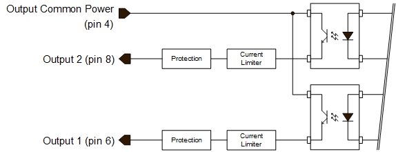
External Output Details and DC Characteristics
-
Programmable output mode such as strobe, event notification, etc. (see outputLineSource feature).
-
Outputs are open on power-up with the default factory settings.
-
A software reset will not reset the outputs to the open state if the outputs are closed.
-
A user setup configured to load on boot will not reset the outputs to the open state if the outputs are closed.
-
No output signal glitch on power-up or polarity reversal.
-
Typical Operating Common Power Voltage Range: +3 V to 28 VDC at 24 mA.
-
Maximum Common Power Voltage Range : ±30 VDC.
-
Maximum Output Current: 36 mA.
External Output AC Timing Characteristics
The graphic below defines the test conditions used to measure the Genie Nano 10G external output AC characteristics, as detailed in the table that follows.
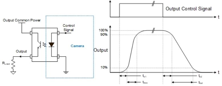
Opto-coupled Output: AC Characteristics
All measurements subject to some rounding.
The following tables describes GPO 1 and GPO 2 when the load is connected to a user-provided ground. Test conditions are with front plate temperature ~62oC, FPGA ~85oC .
|
Output Common Power |
Output Current |
Rload Test (ohm) |
td1 (µs) Leading Delay |
trise (µs) Rise Time |
td2 (µs) Trailing Delay |
tfall (µs) Fall Time |
Vout (V)
|
|---|---|---|---|---|---|---|---|
|
3 V |
8 mA |
240 |
0.459 |
5.03 |
24.07 |
20.41 |
2.17 |
|
12 mA |
144 |
0.492 |
6.95 |
16.9 |
16.35 |
1.75 |
|
|
16 mA |
40 |
0.473 |
4.92 |
9.91 |
10.7 |
0.559 |
|
|
5 V |
8 mA |
523 |
0.469 |
2.64 |
29.22 |
21.33 |
4.24 |
|
16 mA |
159 |
0.485 |
4.75 |
10.96 |
11.14 |
2.57 |
|
|
24 mA |
69 |
0.503 |
6.62 |
7.28 |
8.42 |
1.69 |
|
|
12 V |
8 mA |
1400 |
0.496 |
1.65 |
38.37 |
25.64 |
11.23 |
|
16 mA |
595 |
0.514 |
3.03 |
15.13 |
13.86 |
9.61 |
|
|
24 mA |
360 |
0.531 |
3.76 |
10 |
9.91 |
8.72 |
|
|
24 V |
8 mA |
2907 |
0.541 |
1.63 |
50.75 |
34.39 |
23.31 |
|
16 mA |
1346 |
0.556 |
2.2 |
21.74 |
18.32 |
21.58 |
|
|
24 mA |
861 |
0.567 |
2.5 |
14.61 |
12.93 |
20.72 |
General Purpose Output 3 Fast Switching
GPO 3 supports a fast switching mode with ground of the user load connected to pin 3 (General Input/Output Common Ground). Note, GPO 1 and GPO 2 do not support fast switching. Test conditions are with front plate temperature ~62oC, FPGA ~85oC.
|
Output Common Power |
Output Current |
Rload Test (ohm) |
td1 (us) Leading Delay |
trise (µs) Rise Time |
td2 (µs) Trailing Delay |
tfall (µs) Fall Time |
Vout (V)
|
|---|---|---|---|---|---|---|---|
|
5 V |
8 mA |
561 |
1.69 |
1.2144 |
0.897 |
0.811 |
4.53 |
|
16 mA |
277 |
1.883 |
1.6192 |
0.502 |
0.659 |
4.45 |
|
|
24 mA |
182 |
2.021 |
1.9789 |
0.225 |
0.65 |
4.37 |
|
|
12 V |
8 mA |
1444 |
0.934 |
0.2321 |
2.357 |
0.949 |
11.49 |
|
16 mA |
713 |
0.945 |
0.2563 |
1.759 |
0.369 |
11.41 |
|
|
24 mA |
467 |
0.952 |
0.2739 |
1.481 |
0.224 |
11.33 |
|
|
24 V |
8 mA |
2930 |
0.81 |
0.2079 |
3.542 |
1.639 |
23.57 |
|
16 mA |
1464 |
0.803 |
0.2244 |
2.908 |
0.981 |
23.47 |
|
|
24 mA |
970 |
0.82 |
0.2222 |
2.331 |
0.616 |
23.39 |
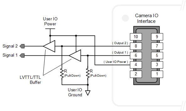
External Outputs: Using External TTL/LVTTL Drivers
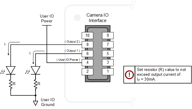
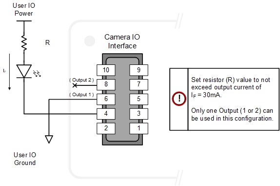
External Outputs: Using External LED Indicators
Two configurations:
-
Two external LEDs can be connected in the Common Cathode configuration.
-
Alternatively, one external LED can be connected in the Common Anode configuration.
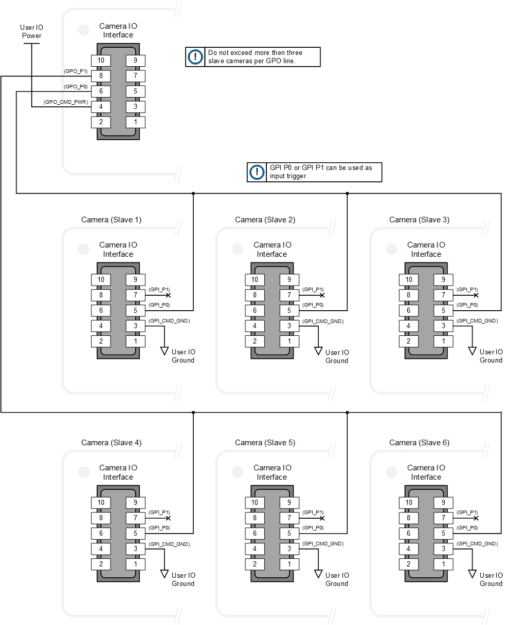
Using Nano 10G Outputs to Drive Other Nano 10G Inputs
A synchronization method where one Genie Nano 10G camera signals other Nano 10G cameras.
| NOTE |
|---|
|
One Nano 10G output can drive a maximum of three Nano 10G inputs, as illustrated below. |
 ©
©